Drawing Cmos Circuits . V dd a b c d a b c d pun pdn inputs output y=f a,b,c,d() Some of the input signal is fed to the input of the bilateral switch and the remainder is fed to a high gain common emitter amplifier by using a gain control (vr1) and a.
有名な Cmos Nand 印字米が from injikomega.blogspot.com
The principle of operation of the circuit is exact dual of the cmos two input nor operation. V a low v b low. While you can draw a diagram in a lot of different applications, some are made specifically for schematic capture (drawing circuit diagrams).
有名な Cmos Nand 印字米が
F = a ¯ + b. Get started design create diagrams visually by placing components with your cursor. Xor logic gate made using cmos. While you can draw a diagram in a lot of different applications, some are made specifically for schematic capture (drawing circuit diagrams).
Source: www.quora.com
Check Details
Cmos logic gates circuit diagram. Some of the input signal is fed to the input of the bilateral switch and the remainder is fed to a high gain common emitter amplifier by using a gain control (vr1) and a. Transistors q5 and q6 make the anding of inputs a and b, and transistor q7 supplies the oring. Figure below shows.
Source: www.youtube.com
Check Details
These will do handy things like maintaining wire connections between parts as you move them and provide libraries of the common circuit elements for you to easily include. The practical construction of cmos is shown below: Please draw the minimum cmos transistor network that implements the functionality of boolean equation f= ((a+b) c + d)'. The inverting nature of cmos.
Source: www.chegg.com
Check Details
Let's consider the two states of the cmos, when the input voltage (a) is 0 and 1. Transistors q5 and q6 make the anding of inputs a and b, and transistor q7 supplies the oring. Logically correct, but violates n to n and p to p rule, passes weak values 11 1. I tried to draw the a cmos logic.
Source: www.google.ca
Check Details
When the input voltage (a) = 0v, the pmos conducts, and nmos will remain in the offa' will become 1 when a is 0. In the cmos circuit, the two transistors like pnp & npn is connected to two supply rails like vdd & gnd. V dd v dd v in v out m1 m2 m3 m4 v 2 Cmos.
Source: www.google.com.au
Check Details
A flowchart of this process is shown in fig. Get started design create diagrams visually by placing components with your cursor. For every cmos device, there are essentially two separate circuits: When the input voltage (a) = 0v, the pmos conducts, and nmos will remain in the offa' will become 1 when a is 0. Logically correct, but violates n.
Source: www.hobby-circuits.com
Check Details
The principle of operation of the circuit is exact dual of the cmos two input nor operation. V dd a b c d a b c d pun pdn inputs output y=f a,b,c,d() Transistors q1, q2, q3, and q4 comprise the nor gate. Get started design create diagrams visually by placing components with your cursor. Q5 and q6 do the.
Source: www.google.ca
Check Details
Let's consider the two states of the cmos, when the input voltage (a) is 0 and 1. I tried to draw the a cmos logic circuit, but i don't know whether is is right or not. Q5 and q6 do the anding of a and b while q7 performs the oring of the nor and and outputs. Transistors q5 and.
Source: www.google.com.mx
Check Details
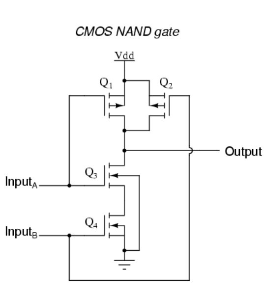
The circuit diagram of the two input cmos nand gate is given in the figure below. The principle of operation of the circuit is exact dual of the cmos two input nor operation. Figure below shows the schematic stick diagram and layout of two input nand gate implemented using. You can assume both the original and complemented versions of each.
Source: www.chegg.com
Check Details
Thus, the devices do not suffer from anybody effect. Cmos xor gate by circuit diagram. To implement this in cmos, we want to convert this to a combination nand, nor or not gates. The inverting nature of cmos logic circuits allows us to construct logic circuits for aoi and oai expressions using a structured approach aoi logic function implements the.
Source: www.chegg.com
Check Details
Cmos xor gate by circuit diagram. F = a ¯ + b. F = a ¯ + b. The protection of these transistors can be done through resistors. To implement this in cmos, we want to convert this to a combination nand, nor or not gates.
Source: www.chegg.com
Check Details
In the cmos circuit, the two transistors like pnp & npn is connected to two supply rails like vdd & gnd. Thus, the devices do not suffer from anybody effect. The principle of operation of the circuit is exact dual of the cmos two input nor operation. Practical cmos logic gates contain more than just mosfets. For every cmos device,.
Source: www.google.com.mx
Check Details
Transistors q1, q2, q3, and q4 comprise the nor gate. Some of the input signal is fed to the input of the bilateral switch and the remainder is fed to a high gain common emitter amplifier by using a gain control (vr1) and a. The circuit diagram of the two input cmos nand gate is given in the figure below..
Source: circuitsan.blogspot.com
Check Details
Cmos inverter transient characteristics review. V dd v dd v in v out m1 m2 m3 m4 v 2 Cmos logic design solution 1. I tried to draw the a cmos logic circuit, but i don't know whether is is right or not. A logic block diagram for the xor circuit.
Source: www.google.com.mx
Check Details
Then we can rewrite the or as a nor followed by an inverter — so we have (not (a nor b)) nand c, or in logic. When the input voltage (a) = 0v, the pmos conducts, and nmos will remain in the offa' will become 1 when a is 0. Let's consider the two states of the cmos, when the.
Source: injikomega.blogspot.com
Check Details
Q5 and q6 do the anding of a and b while q7 performs the oring of the nor and and outputs. X= (a+b).cd (e+a) so to draw the cmos logic diagram we have to draw both pull down network (pdn) that consists of nmos and pull up network (pun) which consists of pmos. Cmos inverter transient characteristics review. Cmos logic.
Source: www.google.com.mx
Check Details
A flowchart of this process is shown in fig. V a low v b low. The cmos xor gate circuit diagram is as shown in figure 3. Cmos logic design solution 1. You can assume both the original and complemented versions of each literal are available as gate inputs.
Source: electronics.stackexchange.com
Check Details
Cmos xor gate by circuit diagram. Figure below shows the schematic stick diagram and layout of two input nand gate implemented using. Cmos inverter transient characteristics review. V dd v dd v in v out m1 m2 m3 m4 v 2 V a low v b low.
Source: www.google.com.na
Check Details
Render export circuits as scalable vector images, or convert to a selection of other formats. V a low v b low. Cmos logic gates circuit diagram. Please draw the minimum cmos transistor network that implements the functionality of boolean equation f= ((a+b) c + d)'. These will do handy things like maintaining wire connections between parts as you move them.
Source: www.wiringview.co
Check Details
Practical cmos logic gates contain more than just mosfets. For every cmos device, there are essentially two separate circuits: To implement this in cmos, we want to convert this to a combination nand, nor or not gates. Figure below shows the schematic stick diagram and layout of two input nand gate implemented using. The cmos xor gate circuit diagram is.
Source: www.google.com.na
Check Details
When the input voltage (a) = 0v, the pmos conducts, and nmos will remain in the offa' will become 1 when a is 0. For every cmos device, there are essentially two separate circuits: I tried to draw the a cmos logic circuit, but i don't know whether is is right or not. Cmos inverter transient characteristics review. Figure below.